Casual Microstrip Design 6
Finally, I get to a post where I can actually attempt to do what I intended to do with the first post in this unintended series. What I will do, Lord Willing, is show a bit of what I have done with a simple microwave filter.
Firstly, I introduce the test equipment I am using to obtain these readings, the NanoVNA V2 Plus4 vector network analyzer. There are many clones in the wild that work okay, but after much reading, I decided to acquire this particular model. Shielding and quality of components are important in a particular piece of test equipment. Otherwise the results may be subject to questioning or random interpretation.
The full specifications for this particular model can be found on the nanorfe website. The following are a select few of the specifications.
- Frequency range: 50kHz – 4.4GHz
- Frequency resolution: 0.01MHz
- Dynamic range: 90 dB or more
- Noise floor: -40 dB or less
Calibration is fairly straightforward. Firstly, setting the frequency range of interest (called STIMULUS). Tapping the screen brings up the menu to select STIMULUS, START and STOP range (or CENTER and SPAN settings). For better resolution, select SWEEP POINTS and set 201. Next, select BACK, then CALIBRATE. Select RESET CAL, CALIBRATE, where a new menu appears to do OPEN, SHORT, LOAD, THRU. Then select DONE and BACK. SAVE the calibration on one of the slots. The User Manual and The Missing Manual are both available on the website.
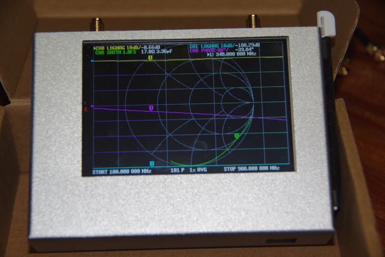
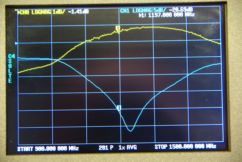
On power up, you see this default screen, with frequency (bottom) set from 100 to 900 MHz. The top lines show the channels (CH0/CH1) where CH0 is Port 1 and CH1 is Port 2. The display is a bit cluttered, but shows some options available for output analysis.
I will use both cables in this particular test, so will calibrate with the two cables connected. So, the OPEN, SHORT and LOAD are connected to the first cable on Port 1 (S11) using the SMA female-to-female ‘barrel.’ The THRU calibration uses the second cable on Port2 (S21) connected to the first cable. After connecting the DUT1, under DISPLAY, TRACE, I turned off all traces except the first two (TRACE 0 AND TRACE 1). Port 1 (S11) is the output signal, and Port 2 (S21) shows the absorption through the DUT. I next adjusted the SCALE/DIV and REFERENCE POSITION settings (under SCALE) to place the traces where I desired. You have to first select the trace you wish to change, then set each appropriately.
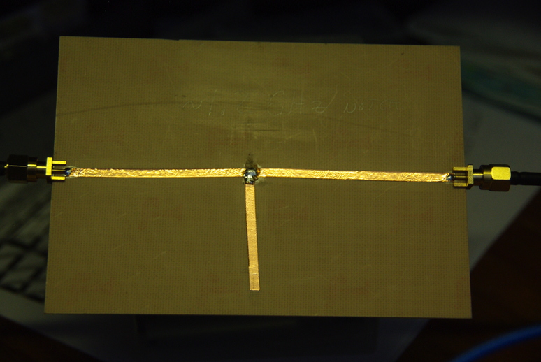
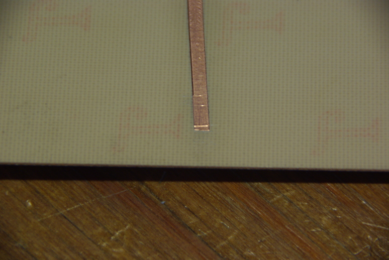
The DUT is connected after calibration, using both cables. This particular circuit in on a single-sided PCB, and consists of stick-on copper tape, normally used for shielding (on guitars, for example.). The total copper thickness is 51 um, including the glue backing. So I suspect it is about 1 oz, or 35 um. The circuit was initially determined using (Wedge, Compton, and Rutledge 1991), then trimmed to tune it a bit. Nothing serious, just playing around for an example.
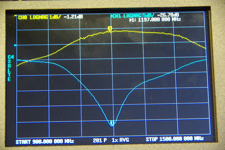
After display adjustment, this is the response through the layout. Moving the marker to the dip shows -26.7 dBM at the tuned frequency of 1.2 GHz with both traces set to a logarithmic scale. I set the SCALE/DIV to 5 dBm per division for CH1, and 1 dBm for CH0. I also moved the REFERENCE POSITION to place CH1 in the best position (#6) for viewing(small blue arrow on left).
The copper tape is really handy for creating a circuit, as it can be trimmed easily. And, the results can be seen instantly on the NanoVNA. Great little tool for quick circuit design. I also checked it against my Tektronix 492P spectrum analyzer, and the results are very similar. The spectrum analyzer shows only amplitude, where the NanoVNA can also show phase. With the scale/div set to 14 and the reference set to 2, I get this display,
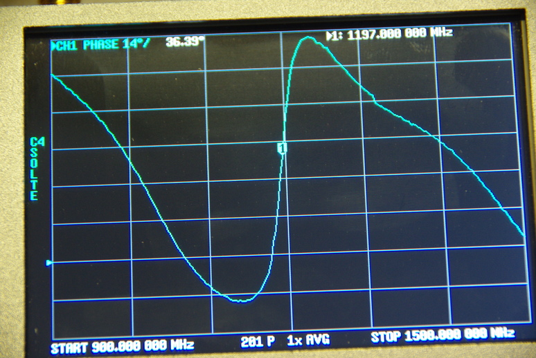
This shows a phase angle of 36o at the marker, and depicts the change as the frequency changes. The below image depicting a Smith Chart, indicates the impedance is a bit higher than the ideal 50\(\Omega\), at 53.6\(\Omega\) with 385 pH of inductance.
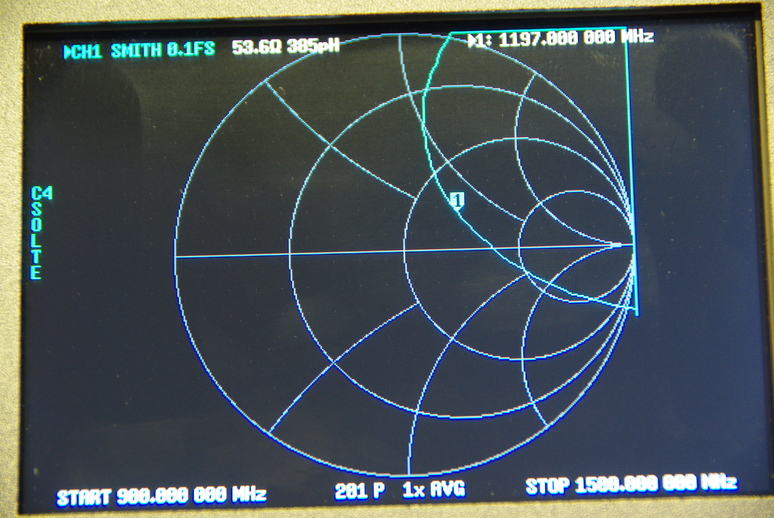
As can be readily seen, the impedance is a bit on the inductive side, and the resistance is high. Some tuning could be done, such as trimming the parallel stub. However, if the copper traces were a bit wider, the impedance might be lower. Trimming the stub would move the frequency. What’s nice with the copper tape is if I trim too much I can just cut another piece and replace the current one.
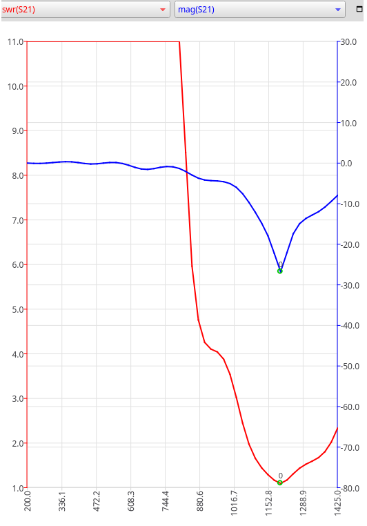
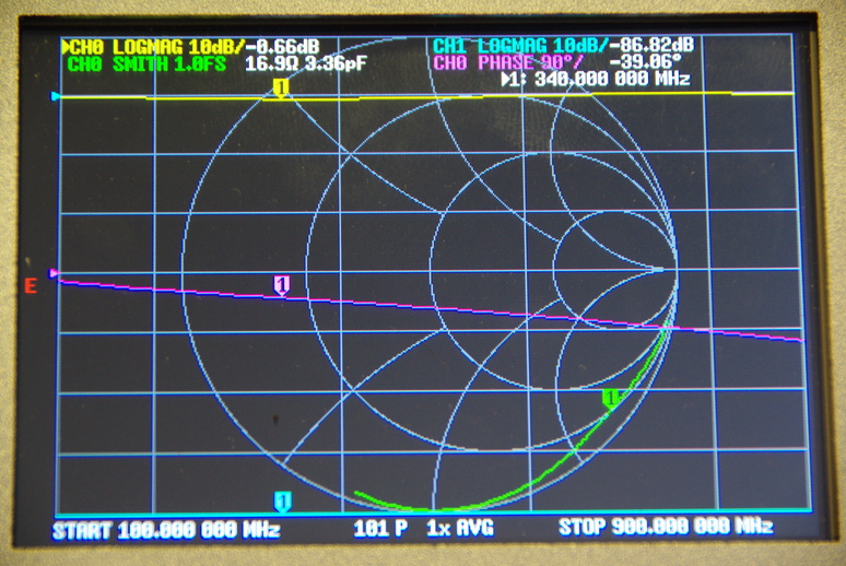
Here, using the NanoVNA software, we have both the SWR and LogMag scales, color coded to match the traces. To see a change, I will trim the stub and see what happens.
The trimmed portion was about one mm. Notice that with just this little bit trimmed off the parallel open stub, the resonant frequency shifted upwards. I didn’t move the below marker, so the shift can be easily seen.
A shift to 1230 MHz is seen in the response, with about -26 dBm dip. The Smith Chart shows 54.5\(\Omega\) with 270 pH inductance, compared with the former values of 53.6\(\Omega\) with 385 pH of inductance.
This was just a quick introduction indicating the ease with which a filter can be tuned, using the NanoVNA. Many more things can be accomplished, and may show up in future postings. Have a great day, and we always praise God for providing!
References
Footnotes
Device under test.↩︎